
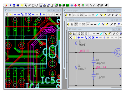
Device design:CAD
● Supports wiring design for a wide variety of electronic devices with different manufacturing environments.
Equipped with functions specialized for designing 3D laminated structures.
Achieves high efficiency in each design work from concept design to manufacturing.
● There is no limit to the layer configuration and library registration that affect the performance of the tool.
You can build your own design for next-generation electronic devices.
● In addition to manual operation using the command menu, automation using the programming function enables users to save time and improve quality.
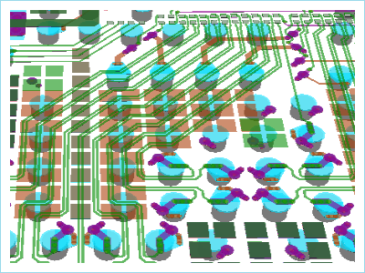
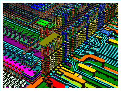
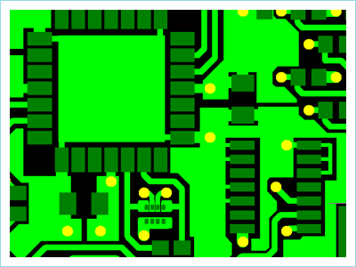
■ Wiring design
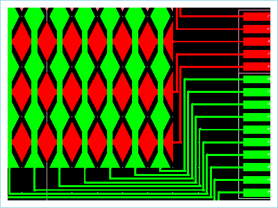
It is equipped with functions for designing various electronic devices such as Si interposers and RDL wiring as well as rigid boards / flexible boards.
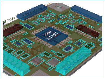
Rigid board design
Unlimited multilayer board
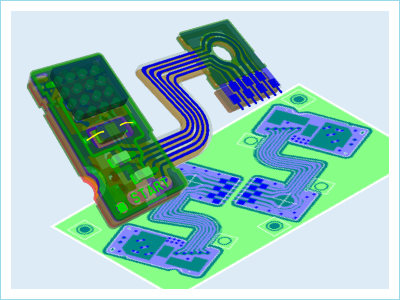
Flexible board design
Unlimited nesting
Silicon interposer
LSI RDL wiring
Other special wiring
Next electronic devices
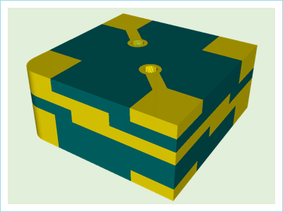
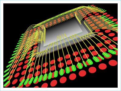
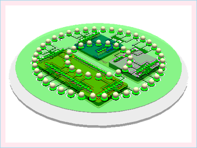
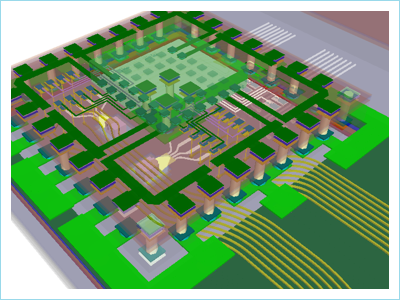
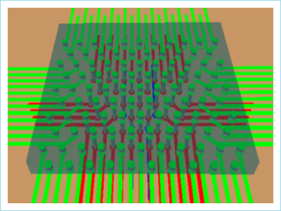
■ Package substrate
We support various package designs due to differences in manufacturing processes.
Chip information can be used smoothly for efficient design.
Various PKG designs
BGA/CSP/FOWLP/POP
Bonding wire
Lead frame
TSV stack
LSI internal connection
Next Generation Packaging
Minimal Fab
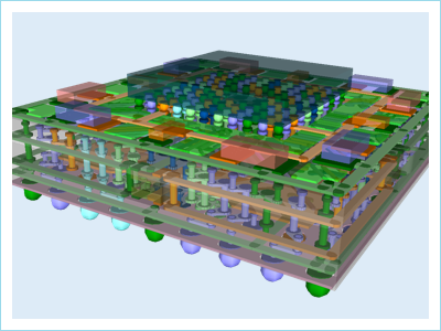
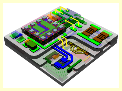
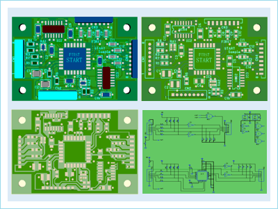
■ State-of-the-art module
You can build a design that fits the structure of a state-of-the-art electronic device.
The layer configuration according to manufacturing can be set freely without any restrictions.
Panel module
FPD/LCD/PDP/EL
Optical and electrical Fusion Module
Co-Packaged Optics Design/Editing/Checking
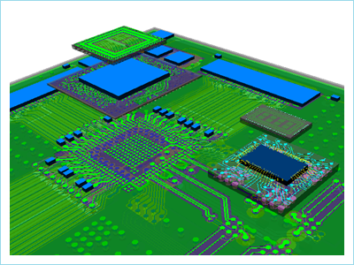
Heterogeneous Module
Chip-Package-Board
Board with built-in parts
Dielectric structure design
■ Specialized function
We support the development of new devices for the next generation and special data processing.
A new style of design is realized by customizing with a dedicated program language.
Restoration of CAD data
Edit attributes
Schematic programming
Coordination with wiring
Reverse engineering
Specialized functions
Programming design
Original language
⇒ Question / Request for materials