
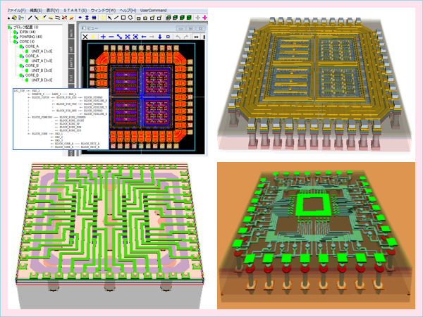
Semiconductor wiring design
Equipped with semiconductor wiring design functions such as RDL manual wiring and TEG wiring.
⇒PWB ~ LSI is linked in a coordinate system that supports mm ~ nm.
It supports input / output of GDSⅡ format, and new design & editing can be carried out.
⇒ It can be used as a support tool for LSI design, such as 3D conversion of GDSⅡ data and simple CMOS wiring.
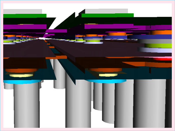
◆ The LSI pattern can be simplified and converted and used as a SIM verification model.
◆ Connection can be verified by stacking module synthesis by TSV.
◆ It is possible to automatically create TEG patterns etc. using the programming function.
※Please Contact us for details.