
Company Information
| Company Name | FIRST Co., Ltd. |
| representative | Kazuharu Baba |
| Headquarters address | 4-18-4 Ikejiri, Setagaya-ku, Tokyo 154-0001 [ Access map ] |
| Capital stock | 10 million yen |
| Established | August, 1988 |
| Fiscal year end | July |
| Major banks | Sumitomo Mitsui Banking Corporation |
| Business Content | Development and sales of "START"—the world’s first EDA tool featuring integrated CAD/CAM programming—along with version upgrades, operational support, foundational and practical training, and customization services (including the implementation of proprietary technologies and the centralized control of manufacturing equipment). |
会社沿革
| August 1988 | Establishment |
| October 1991 | Release of the world's first CADCAM fusion tool, 'START'. |
| October 1995 | Equipped with expanded design and editing capabilities for FPC/COF/TAB |
| July 1996 | Expand and equip subscription design and editing functions. |
| April 1998 | Expanded and equipped with GDSⅡ format input/output and editing capabilities. |
| December 2006 | Expansion and integration of design, editing, and inspection capabilities for FPD (LCD/PDP/OLED) panels and PWBs. |
| March 2008 | Supports standardized analysis models, including ANF, SPD, XFL, IDF, LAY, S3D, etc. |
| September 2009 | Implementation of 3D integration, inspection, and modeling for LSI/PKG/Board under the national project "ASET". |
| May 2010 | Comes with Sef (Start Execute Format)—a programming language for customization—as a standard feature. |
| December 2012 | Initiating custom direct control for manufacturing equipment (laser processing machines, exposure systems, mounting machines, and inspection equipment). |
| December 2013 | Implemented in the national project "PETRA" for optoelectronic integration design, editing, inspection, and modeling. |
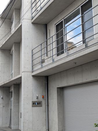
| May 2014 | Construction of a company-owned building. |
| April 2018 | Implemented for design, inspection, and modeling of 3D ICs using quantum annealing—part of a national project. |
| August 2020 | ndustry-first: Launch of the DEMITASNX interactive (two-way) interface. |
| March 2023 | Implemented for 3D packaging design, inspection, and modeling at the Semiconductor Research and Education Center, Faculty of Advanced Science and Technology, Kumamoto University. |
| September 2026 | Implemented at Chitose Institute of Science and Technology, a constituent organization of the Leading-edge Semiconductor Technology Center (LSTC) research association. |
| Conclusion of a joint research agreement regarding design rules for CPO (Co-Packaged Optics) in next-generation semiconductors. |
主な導入ユーザー
イビデン(株) 日本サムソン研究所(株) ルネサスエレクトロニクス(株) (株)ミクロ技術研究所 デバイステック(株) アムコーテクノロジージャパン(株) (株)デンソー (株)ニコン (株)ミクロ技術研究所 タツタ電線(株) 日本電気(株) (株)大昌電子 コネクテックジャパン(株) タカノ(株) ヌヴォトン テクノロジージャパン(株) パナソニック(株) 信越ポリマー(株) キヤノンプレシジョン(株) キヤノン(株) メイコー(株) 日本発条(株) 帝国通信工業(株) シャープ(株) (株)日本マイクロ二クス スタンレー電気(株) 山一電機(株) 日東電工(株) (株)ワコム 東レエンジニアリング(株) アテネ(株) 住友電工プリントサーキット(株) 山下マテリアル(株) (株)アルファー精工
Track record of implementation by national projects and educational institutions
・ASET (Association of Super-Advanced Electronics Technologies) Dream Chip Project
・PETRA (Photonics Electronics Technology Research Association) Research Institute for Photonics-Electronics Convergence
・5G Project: Integration of Quantum Annealing with 3D Stacking and Packaging Technologies
・Research on Low-Noise Technologies for LTE-Class RFICs
・Development of Ultra-Low-Loss Power Devices
・Development of Ultra-Low-Power-Consumption Optoelectronic Packaging System Technologies
・Semiconductor Research and Education Center, Faculty of Advanced Science and Technology, Kumamoto University
・Joint Research on Photonics-Electronics Convergence with Chitose Institute of Science and Technology (a member institution of LSTC)