
New semiconductor packaging system
We support the development of next-generation semiconductor manufacturing equipment.
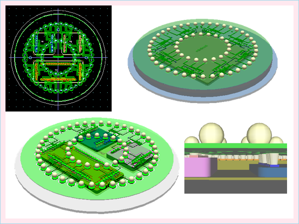
■ By designing and editing the GDSⅡ system, the wiring data of the LSI can be converted into 3D data.
■ It corresponds to laser type NCVIA with thickness information added.
■ With the programming function, you can build a new cooperation format.
◆ Minimal Fab https://unit.aist.go.jp/kyushu/minimallab/
※Please Contact us for details.